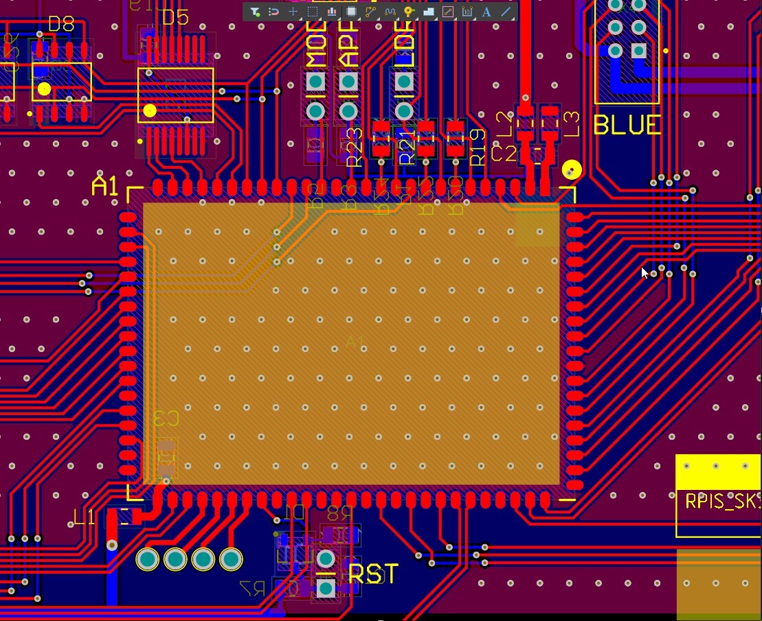
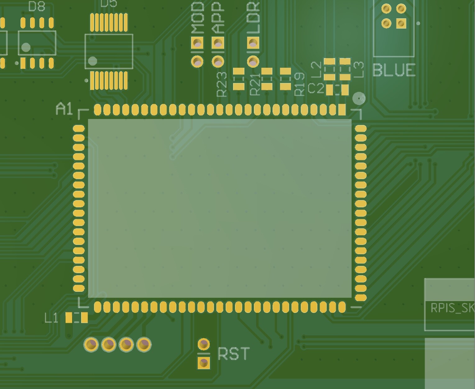
According to the SitCore SOM datasheet says, “We recommend no traces or vias under the module.”
How hard and fast is that recommendation? I assume it is just traces on the top layer directly under the module and traces can be on the internal and bottom layers? (It is a 6 layer board.) Have others put traces or vias under the module?
On one of my boards i followed the recommendation and didn’t put them. On another i just couldn’t squeeze them anywhere else. The second board arrived but haven’t tested it yet, to see if there is an issue with that. So im curious as well.
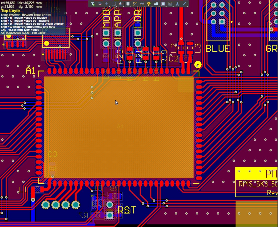
I have not worked with the SITcore SOMs but have worked with the G120 and G400 in the past and almost always had vias en signals routed directly underneath them.
Nowadays, I mostly use the SC20100S in LQFP package and I never had any problem with having vias or signals underneath them.
The only thing I like to keep free from any disturbance is my main crystal. I have had bad experiences having other signals going underneath the crystal, both top and bottom layers. I usually try to keep signals away from the crystal and sometimes I go the extra mile and protect my crystal with a ground ring.
In conclusion, I don’t think you’ll find any problems routing signals underneath your SOM. There might be exceptions, like if you’re planning on using SPI or similar on super super high clock frequencies, then it might cause problems.
There are very slim chance of having issues. And if you limit how much you have under it then your chances of having issues are very very very very slim.
How many “very” is good for your needs is up to you.
The largest concern comes from environment with high vibration and significant temperature changes, most of us do not have these environments so you are fine.
I’ve done this since the G120 days and recently with the SITcore without any issues.
I just make sure that all via’s are tented so that they are covered in solder mask. The modules themselves also appear to be tented so you get double protection.
It is theoretically possible to short-circuit via vias due to uneven solder mask coverage of both the module and your board.
However, I do the same as @Dave_McLaughlin - cover vias on my board plus add silkscreen under the module and get triple protection. Also, no problems with either the G120 or the SCM20260N. Not a single failure or short circuit during the entire application.
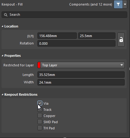
I am using Altium, so I will only tell you for it. Specifically, I have version 20, it should be similar for previous versions.
There are two ways:
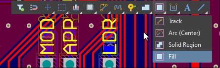
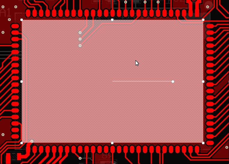
Dreary. Let’s do the Via Stitching, then manually delete each via under the module. We repeat the procedure after each correction.
Logical. We put the keepout region under the module and leave the restrictions only for vias in the settings. If there was a Via Stitching, then it will need to be deleted and recreated.
@LucaP
I agree. I currently use Eagle and I still feel like I am back in the 1990’s when I use it.
I almost made the jump to Altium last year but I have so much time invested in Eagle it is hard to make the switch.