Can I delete the things I do not need like the LED part? Also I am unsure of some parts in bold below (hopefully I did the rest correct):
// constants
//
// System clock
#define SYSTEM_CLOCK_HZ 84000000 // 84 MHz
#define SYSTEM_CYCLE_CLOCK_HZ 84000000 // 84 MHz
#define SYSTEM_APB1_CLOCK_HZ 42000000 // 42 MHz
#define SYSTEM_APB2_CLOCK_HZ 84000000 // 84 MHz
#define SYSTEM_CRYSTAL_CLOCK_HZ 12000000 // 12 MHz external clock
#define CLOCK_COMMON_FACTOR 1000000 // GCD(SYSTEM_CLOCK_HZ, 1M)
#define SLOW_CLOCKS_PER_SECOND 1000000 // 1 MHz
#define SLOW_CLOCKS_TEN_MHZ_GCD 1000000 // GCD(SLOW_CLOCKS_PER_SECOND, 10M)
#define SLOW_CLOCKS_MILLISECOND_GCD 1000 // GCD(SLOW_CLOCKS_PER_SECOND, 1k)
#define SUPPLY_VOLTAGE_MV 3300 // 3.3V supply
// Memory
#define FLASH_MEMORY_Base 0x08000000
#define FLASH_MEMORY_Size 0x00080000 // 512K
#define SRAM1_MEMORY_Base 0x20000000
#define SRAM1_MEMORY_Size 0x00018000 // 96K
//total GPIO PORTS A,B,C,D
#define TOTAL_GPIO_PORT 3
#define TOTAL_GPIO_PINS (TOTAL_GPIO_PORT*16)
//total UART TLL ports
#define TOTAL_USART_PORT 3
#define USART_DEFAULT_PORT COM1
#define USART_DEFAULT_BAUDRATE 115200
//used generic but SWO is PB3 it should defined otherway … on nucleo stm32f411ret6
#define TOTAL_GENERIC_PORTS 1 // 1 generic port extensions (ITM channel 0 )
#define ITM_GENERIC_PORTNUM 0 // ITM0 is index 0 in generic port interface table
//debug to be used …
#define DEBUG_TEXT_PORT ITM0
#define STDIO ITM0
#define DEBUGGER_PORT USB1
#define MESSAGING_PORT USB1
//total controllers
#define TOTAL_USB_CONTROLLER 1 // FS only
#define USB_MAX_QUEUES 4 // 3 endpoints (EP0 + 2)
//scok port
#define TOTAL_SOCK_PORT 0
// System Timer Configuration
#define STM32F4_32B_TIMER 5
#define STM32F4_16B_TIMER 1
// Pin Configuration
#define STM32F4_ADC 1
#define STM32F4_AD_CHANNELS {8,9,10,11,14,15,16,17,20,21,22,23,24,25,26,27} // PC0, PC1, PC2, PC3, PA0, PA1, PA2, PA3, PA4, PA5, PA6, PA7, PC4, PC5, PB0, PB1
//pwm
#define STM32F4_PWM_TIMER {2,2,2,3,1,1, 1, 1, 2, 2, 3, 3, 4, 4, 4, 4, 2, 3, 3, 3, 3}
#define STM32F4_PWM_CHNL {1,2,1,1,1,2, 3, 4, 1, 2, 1, 2, 1, 2, 3, 4, 3, 1, 2, 3, 4}
#define STM32F4_PWM_PINS {0,1,5,6,8,9,10,11,15,19,20,21,22,23,24,25,26,38,39,40,41}
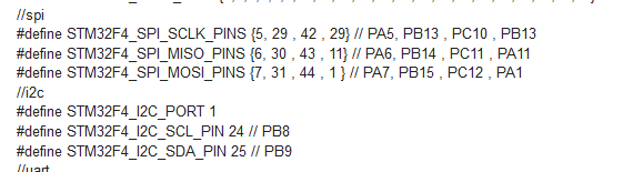
//spi
#define STM32F4_SPI_SCLK_PINS {55, 34} // PB3, PB13
#define STM32F4_SPI_MISO_PINS {56, 35} // PB4, PB14
#define STM32F4_SPI_MOSI_PINS {57, 36} // PB5, PB15
//i2c
#define STM32F4_I2C_PORT 1
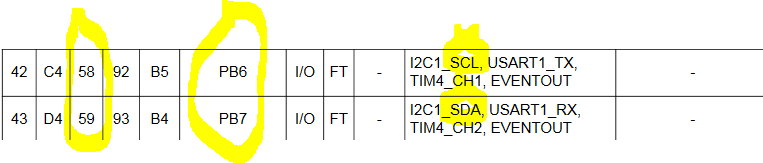
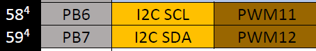
#define STM32F4_I2C_SCL_PIN 58 // PB6
#define STM32F4_I2C_SDA_PIN 59 // PB7
//uart
#define STM32F4_UART_RXD_PINS {43, 17} // PA10, PA3
#define STM32F4_UART_TXD_PINS { 42, 16} // PA9, PA2
#define STM32F4_UART_CTS_PINS {GPIO_PIN_NONE, 14 } // PA0
#define STM32F4_UART_RTS_PINS {GPIO_PIN_NONE, 15 } // PA1
// User LEDs
#define LED2 5 // Green
// TinyBooter entry using GPIO
#define TINYBOOTER_ENTRY_GPIO_PIN 45 // User button
#define TINYBOOTER_ENTRY_GPIO_STATE FALSE // Active low
#define TINYBOOTER_ENTRY_GPIO_RESISTOR RESISTOR_DISABLED
//
// constants