Hello my friends,
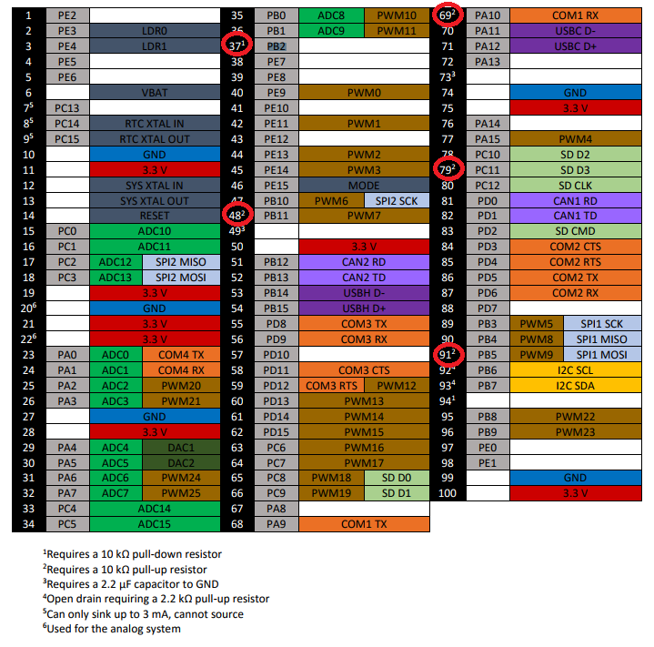
I have prepared my own PCB with G80 and of course I did not include pull-up/down resistors from datasheet. But my pcb is working (I am not using those pins), my question is … what I am I losing besides functionality on those pins ? The most mysterious is pin 37. Is it necessary to apply them even if I am not using it ? I marked those pins on attached photo. Thank you in advance !
You really need to follow the manufacturer guidance here - find a way to add the resistors to your existing PCB. The reason they are listed is because they control behaviours in the PCB, and without controlling that with PU/PD resistors you’re risking startup issues
69, 79 and 91 are not required if you are not using those ports for their intended use, eg 69 is COM1 and if not using, don’t need this pullup, 79 is SD card so if no SD card in your design, not required and lastly, 91 is SPI so again, if not using the SPI port, no need for a pullup. The same applies to SDA and SCL. If you are not using that feature, no need for any pullups.
37 and 48 I would add regardless as they are used by the bootloader as far as I can tell.
Thank you gents for help, Next time I will add those resistors but since my PCB is working I would like to know if I can install my device on the field,this time I am too lazy to prepare new PCB Thank you Dave for help, you confirmed my predictions.
If you don’t pull up 37 and 48 you may find that occasionally your device will enter the bootloader instead of your application. Something may change, even just the environment the device is operating in, and it may start failing at higher frequency. Better to place them now than add it to the list of potential support issues.
Or maybe everything will be fine… gathering statistics on the risk may be difficult, but you can consider what the cost would be for hypothetical rates of failure.
Botch wires with resistors would fix the issue without redesigning the PCB. Would have to weigh that against the increased cost/time of manufacture and risk of breakage due to mechanical vibrations.
I think you are right. The circles in the diagram are next to the pins that are generally pulled up or down… but on the wrong side. The pin numbers are 2 and 3.
From previous experience, LDR0 and LDR1 have never required a pull up and just need a link or switch to GND to activate them. They have internal pullup to ensure that the pins are in the correct operating mode. The other pins I mentioned above are required when using them as anything other than GPIO.
 Thank you Dave for help, you confirmed my predictions.