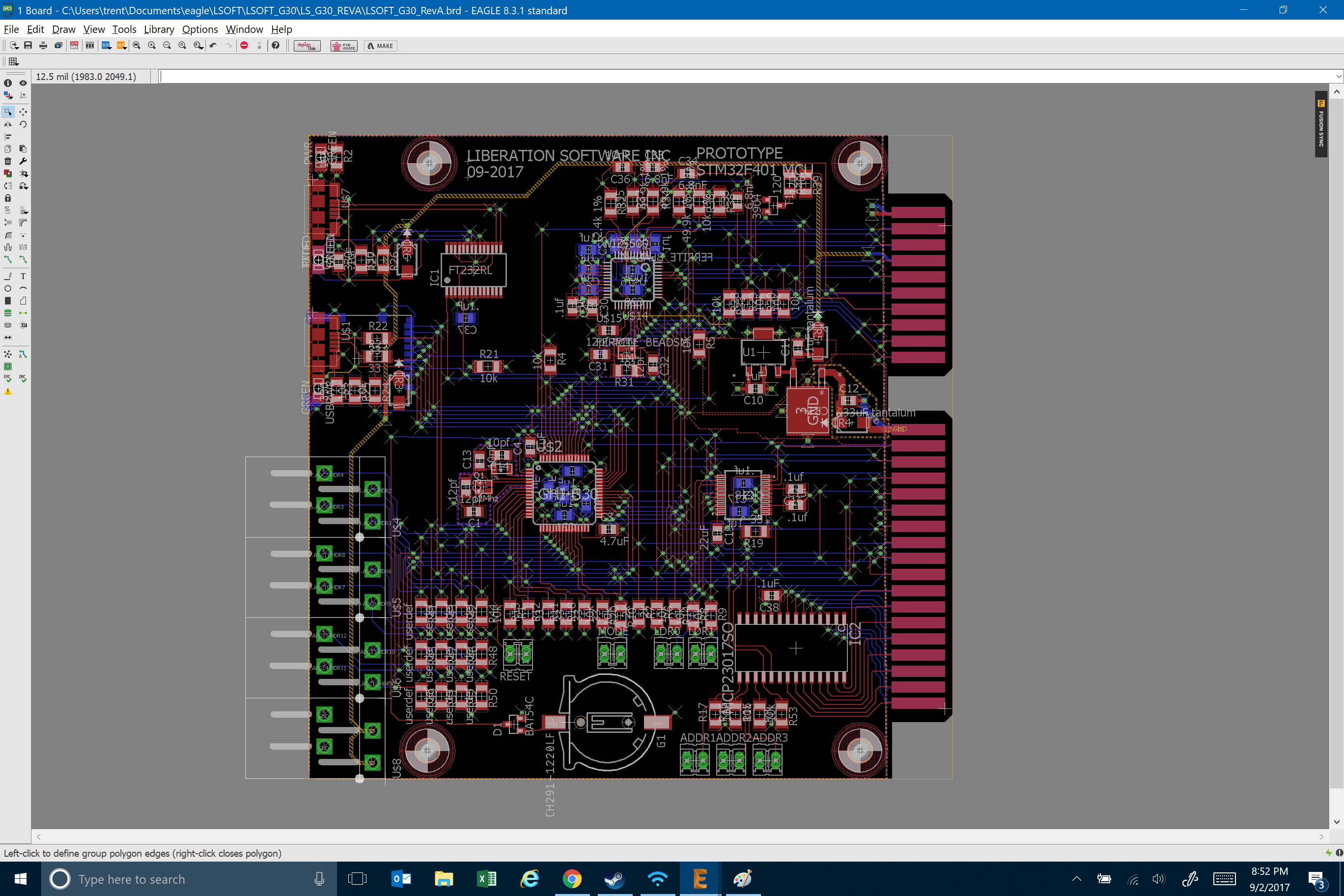
On VCC I didn’t pour a plane as I wanted to ensure caps were connected in specific order. Bigger chip decouplers feeding the individual .1 decouplers on pins, etc. Pullups are on the main 3v3 line, not the board line.
I figure that way signals won’t “screw” with my chip.
I also have for the wiz5500 separated out the path for 3v3 analog and digital and kept them completely separate on routing past the ferrite beads.
Hoping to have no noise at all.
The last prototype board I did, I had incredibly clean 3v3 to certain parts of the board but others were very noisy on the scope, as I did VCC and ground all willy-nilly and haphhazardly.
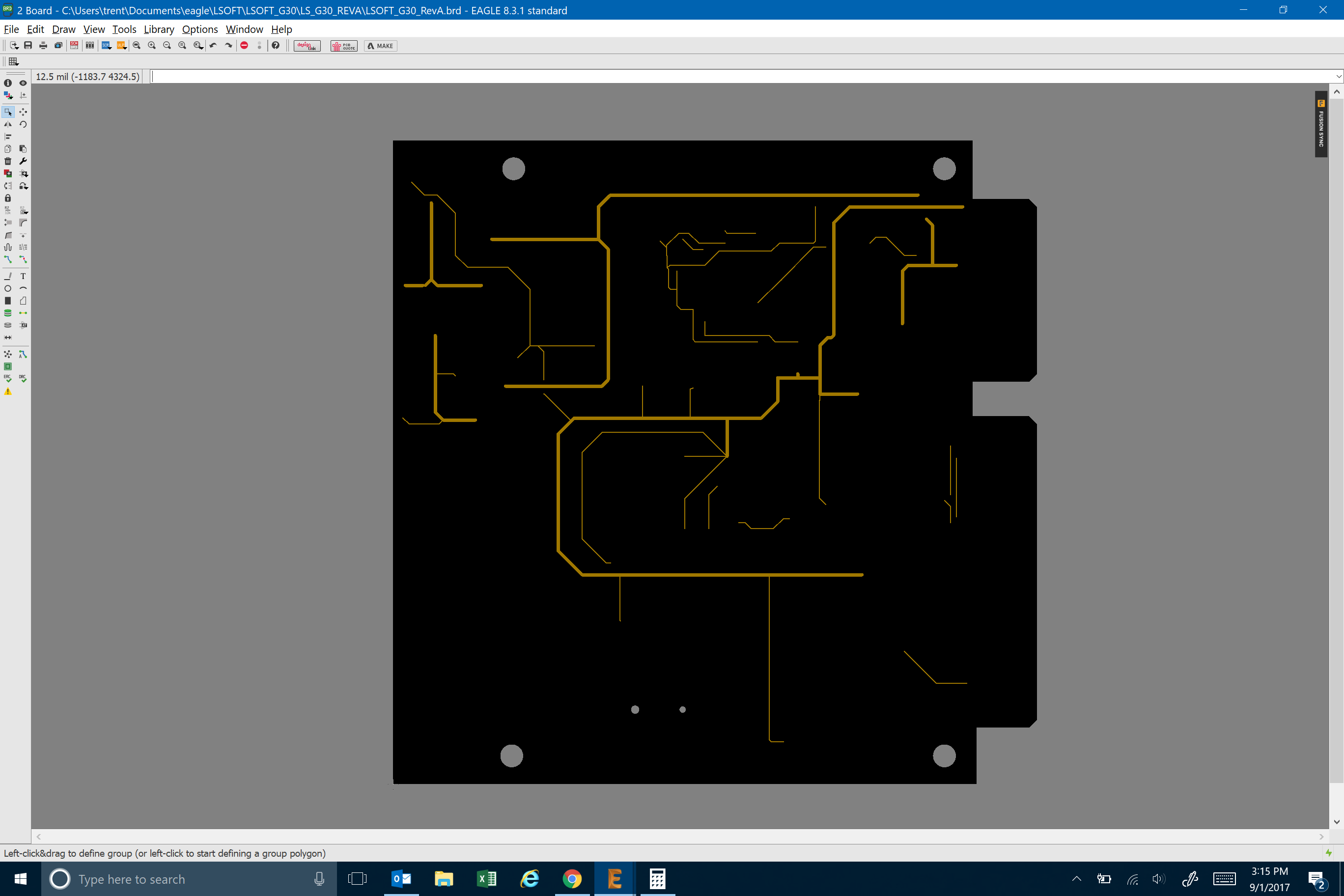
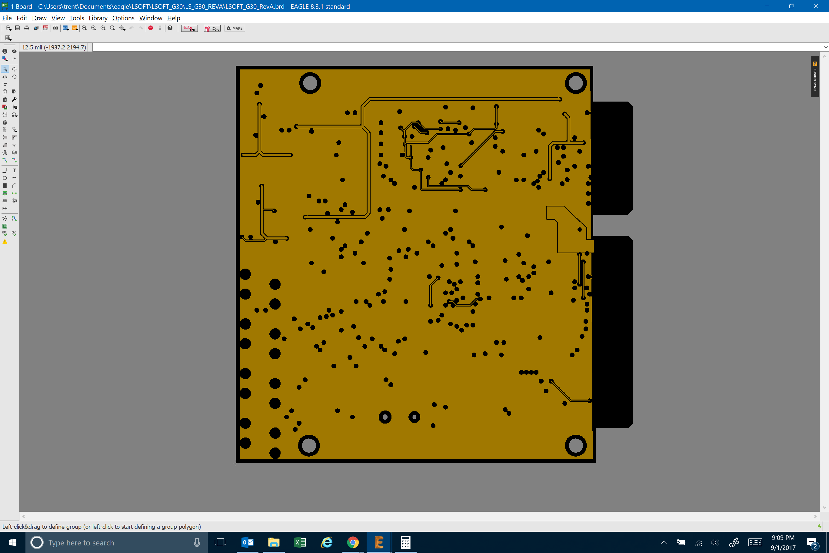
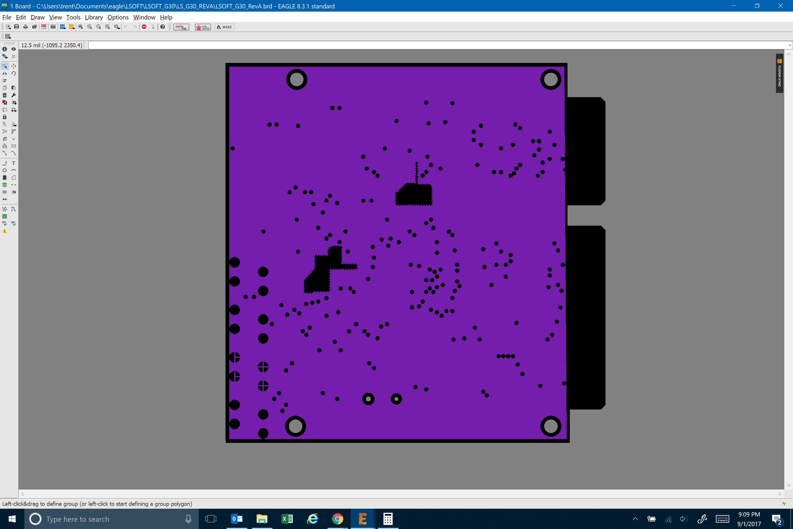
Here’s the isolated VCC and ground planes.
(top and bottom of inner core on the stackup)
Managed to keep signals on the top and bottom of the board, only borrowed voltage layer for a couple of things
I know this is venturing off in to non-compute module stuff but that TI whitepaper I read on EMI (think I linked to it a ways above) mentioned creating a floating plane to shield the oscillator. This should stop it from sending noise in to the signal traces below it? I have some analog inputs run underneath the thing. There was just no way to route them around. I managed to avoid routing any high speed (USB, SD, SPI) signals anywhere near an oscillator but those analog lines are right smack underneath it.
So something like this?
Another oddity. Having put 24+ hours in to a design in a 30-ish hour real world time window, when I finally did catch some ZZ’s (Zeds, to you Canadians), I actually dreamed of routing traces.
Well, it was more like a nightmare because in my dreams I couldn’t get one last trace broken out and connected.
Like any visual repetitive task the ‘art of laying down nets’ is one that really creeps in to your subconscious.
1 Like
Did some more reading.
I moved my analog signals from under those oscillators. Only took a half hour to reroute.
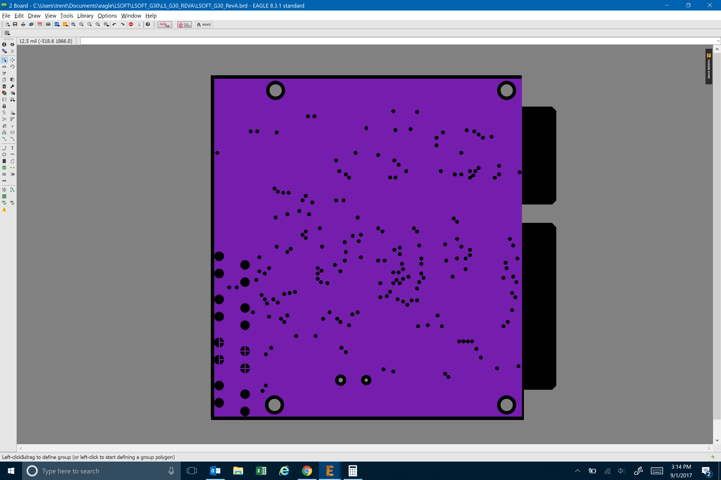
@Mr_John_Smith I also changed my VCC layer to be a fill. Won’t really change anything, except the core will be less likely to warp, now that there are equal pours on both sides.
Also cut out the ground plane under the oscillators. Probably should do the same to VCC layer I imagine? Eliminate any capacitative coupling from the oscillators.
Yeah I know, not a circuit design forum 
But relevant for anyone doing signals on a board that uses IC’s with an external oscillator. (Got three in this case, 25mhz, 12mhz, and 32768hz)
2 Likes
Typically, on a 4 layer board where I have an oscillator I leave the inner planes as they are and add a floating ground plane around the crystal on the top layer. With 4 layer boards I typically never flood the top and bottom unless I have a lot of analog signals and then I place a row of guard via’s around the edge. You typically see this if there is any RF sections on a board. For most of the stuff we do, not really necessary although it does look cool 
2 Likes
Well I did a check through everything and realized I’d forgot voltage divider resistors for my analog inputs on the left side. Kind of hard to calculate R2 without the R1 value on an ADC…
4 1/2 hours later… sigh…
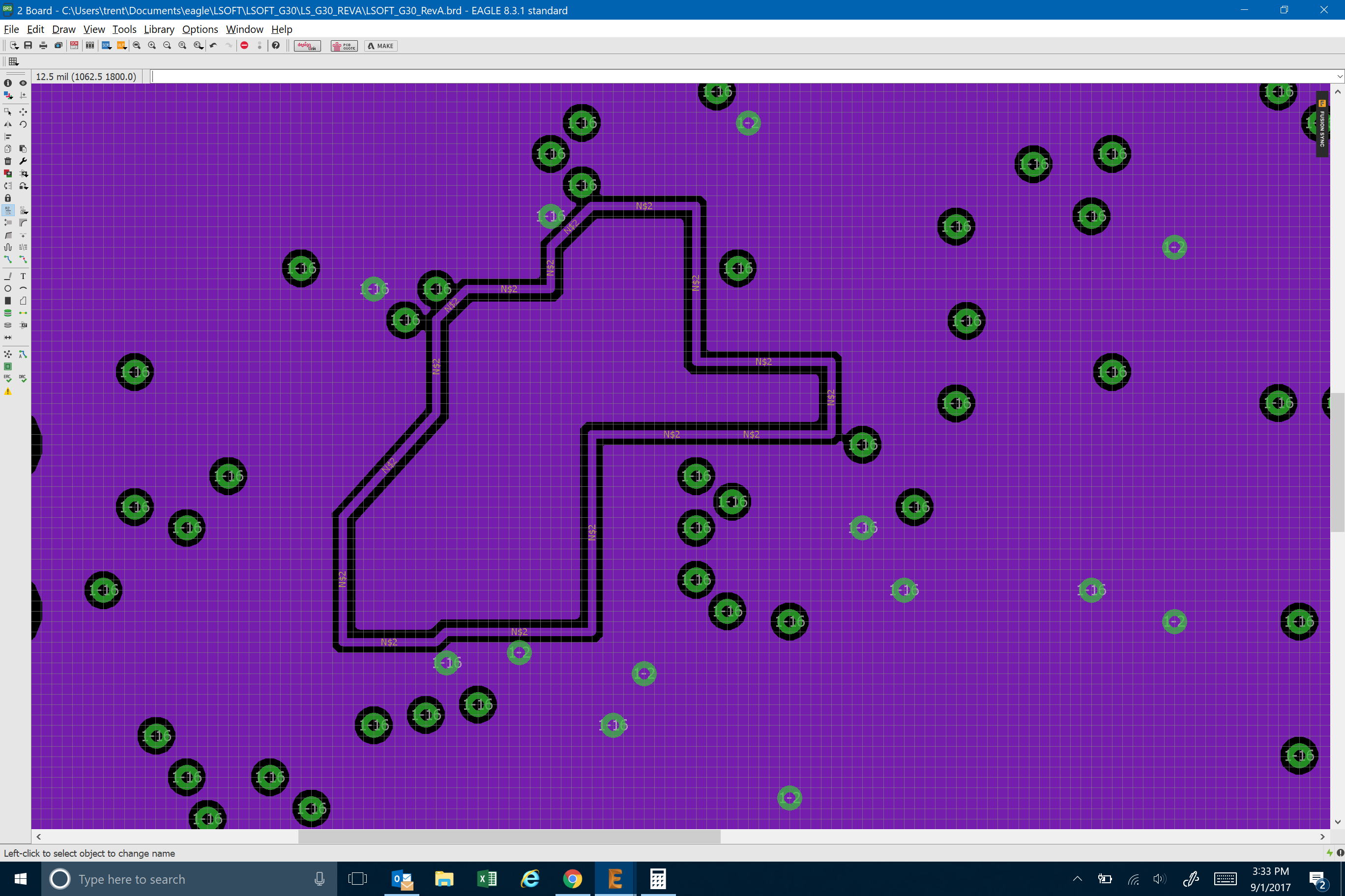
It also occurred to me that pull-up / pull-down resistors don’t need to be sitting close to the IC, and that anywhere along the signal line will do. So that cleaned up the board immensely.
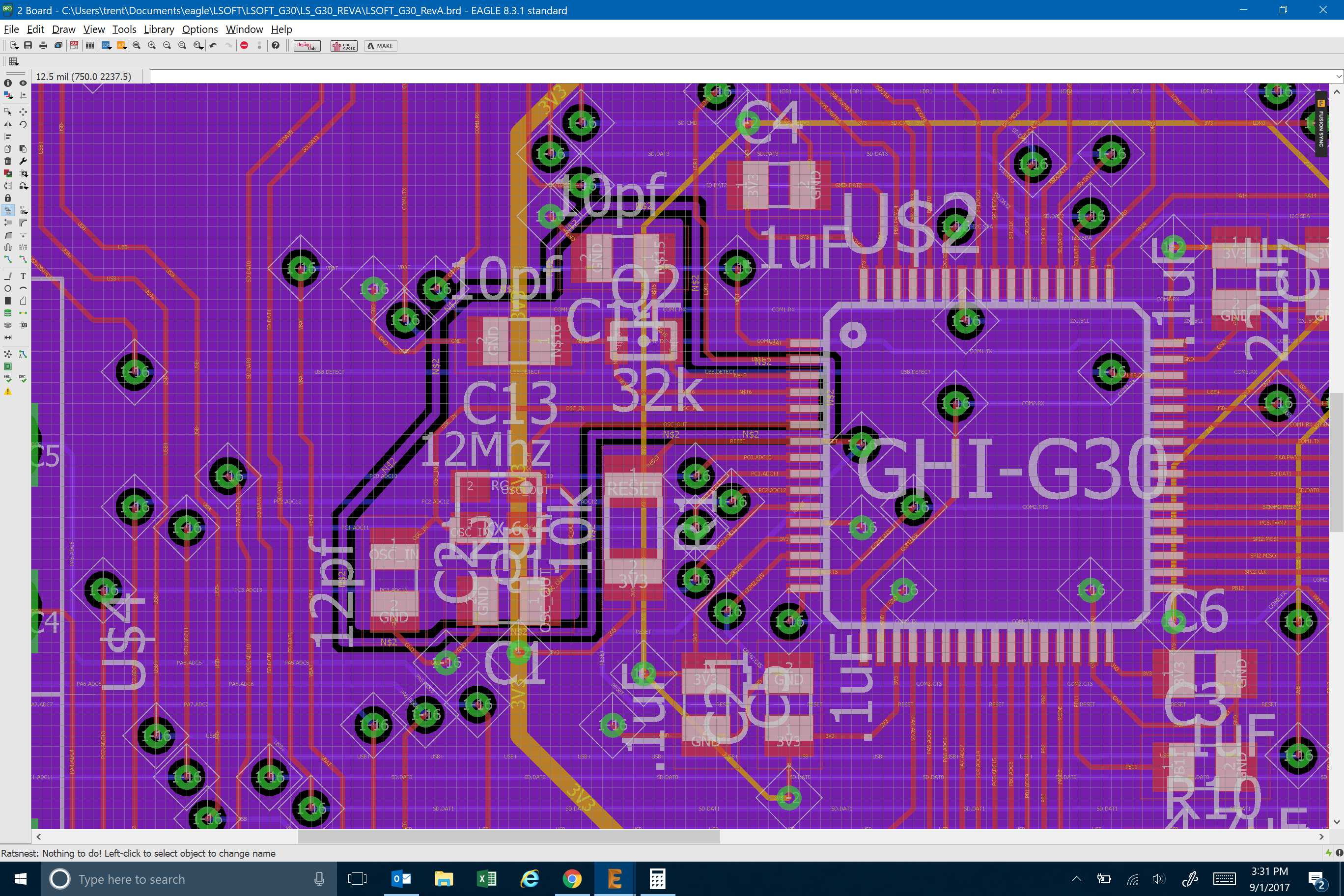
I also moved a lot of the IC capacitors to the back side to clean up signal breakout, and did a better job on gridding my signals.
It looks a LOT cleaner now.
Oh and thanks for the tips, Dave. I’m curious to see how clean these analog lines are once it gets made.
Each time I ripup !; I about cry. But I’m pretty happy with where this one ended up, only took 3 tries.
Good thing I did the sanity check this afternoon.
Aside from the ADC voltage divider resistors, I’d also forgot a pullup resistor on the reset line of the GPIO extended I am using. That would have been frustrating to diagnose!
1 Like
I think you made a good choice moving the ADC lines away from your oscillator. I recently went through a redesign because I had some ADC signals near an inductor helping to switch power down from 5V to 3.3V.
My motor (whose position is read on those ADC lines) loved to fluctuate ever so slightly, giving me a nice audible indicator of what duty cycle my RGB LEDs (feeding off the 3.3V rail) were running.
@trent1098s I am having the same issues as you did where the G30 shows up in Device Manager but won’t connect in FEZ Config. Can you please walk me through how you got past this part / where do I find the FW files you loaded with Tera Term/how do I do that part?
See my post here for more details.
The firmware file was under Program Files (x86)\GHI Electronics… Look for G30 and you want to send Firmware.ghi up.
Make sure you configure the xmodem protocol properly in terraterm you want 1k frames.
The path that I went down followed their documentation here.
http://old.ghielectronics.com/docs/54/loader-tinybooter-g120-and-emx-families