When deployment to my G30 is unsuccessful my board enters a strange state in which my 3.3 V rail rises to 4.0 V, rapidly switching on and off. This power is ultimately coming from my separate 18 V rail, but I’m having trouble figuring out how this connection is made.
What state is a G30 put into when deployment fails? What are the pins doing?
Edit: After further testing, I have removed a USB power switch and now I cannot recreate the problem. This makes me particularly interested in what happens to VUSB when the deployment fails, or even during deployment. VUSB is not actually connected to the USB cable I am programming with in this scenario.
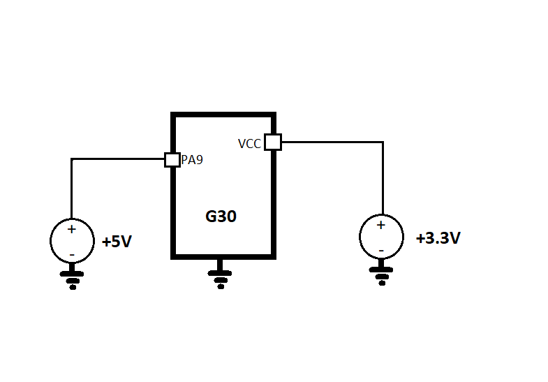
I’ve explored the exact problem and I think the schematic does not need to be more complicated than this:
I see that PA9 is “5V Tolerant” but I don’t know if that somehow applies to the pin in Output HIGH state. I already see that the 3.3V rail will actually rise to about 4 V, and things don’t work. But it’s a corner case because it only happens if deployment fails.
My actual question is if this okay and will not cause damage to the G30?
So a 3v3 regulator should regulate voltage to only allow 3v3, not allow it to creep to 4v. That should be the “limit” to all this. If you have something weird in your circuit that goes out of spec, say for example when something draws too much current, then that’s your circuit’s issue not the G30’s.
5v tolerant is the input condition. It means that if the input you’re sensing is a 5v source, you won’t blow things up. Contrast that to a pin that is not 5v tolerant, if you are sensing a 5v source you will destroy the pin/micro. In an output sense, it can only output 3v3, or the operating voltage of the micro (ie it can’t boost to 5v). If you have PA9 connected to the 5v supply rail like you show, it’s unnecessary, but unlikely to cause you issues, but if you are also using it as an output pin then that’s a short circuit between the 3v3 and 5v circuits, and certainly could lead to trouble.
Why don’t you share your actual circuit? If you’re concerned about your issue, more eyes helps - if you’re not concerned, then …
Here’s the one thing I would say. If you have PA9 connected to the 5v rail with no current limiting, and you put the micro in reset (like programming it would), your code is no longer working and the pin state will revert to whatever the manufacturer wants it to. That could well be an input of some kind, and internally that’s causing back leakage into VCC and showing an apparent ~4v on the VCC pin. So why do you have PA9 to 5v? And do you have current limiting? (see how easy both those questions would be if we saw the schematic?)
I suppose sharing this schematic does bring some new information to the table.
I have control over whether I supply 5V to PA9 by controlling PC0 with code. Default: Not supplying 5V
I do not have control over a person supplying 5V to PA9 with an external device.
I think it is important to note that while I am not actively using PA9 as an output, it appears it can be configured as an output (due to some underlying software) when deployment fails.
I would use a current limiting resistor on PA9 as an input pin, as you’re possibly exposed to higher than 5v momentarily on a noisy line and that alone is worth protecting with a resistor. I’m assuming that this is just to sense when there’s USB bus power on the external connector?
Also, since you know it’ll be 5v and you only want to sense 3v3, you could consider properly protecting it with a voltage divider to still give you peak voltage over the micro’s high-sensing voltage (2.4v? check the datasheet) Anyway, significantly less than 3v3, so a pair of reasonably closely matched resistors will get you in the ballpark.
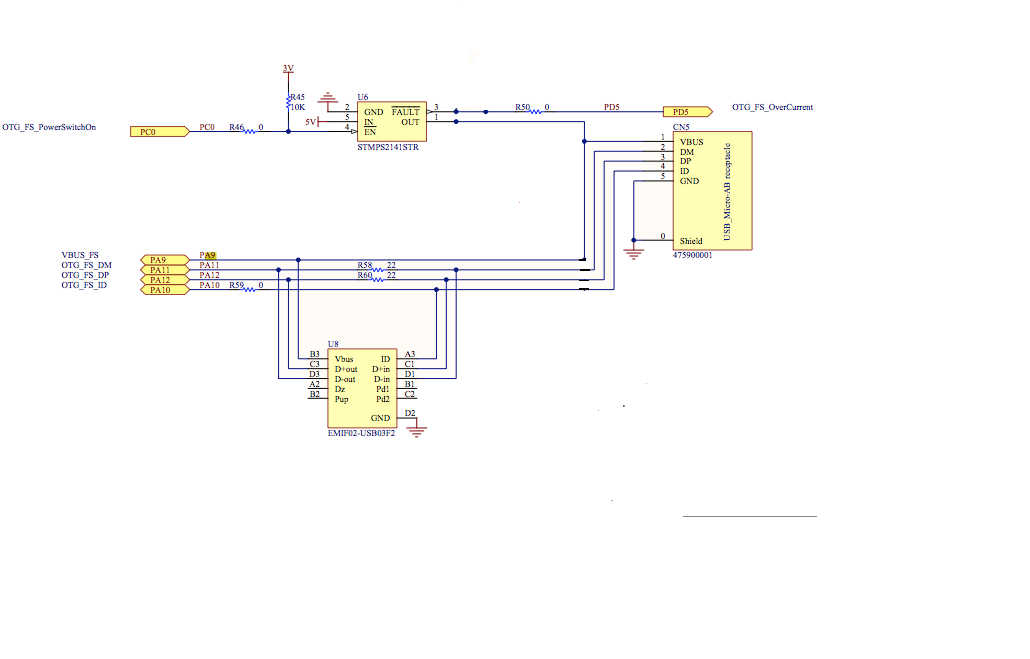
Is that the default/suggested schematic for the EMI protection chip? I would have expected it to break D+/D- lines, but didn’t look…
Thanks for the suggestion that may be all that is needed. I think I will throw in a diode for good measure.
This schematic comes straight from ST. Not meant for NETMF I don’t believe however.
About the EMI chip’s schematic: It eludes me why there is the 22 ohm on each data line in parallel with the 33 ohm internal to the chip, but whatever… it works. Turned out to be a stroke of luck when my first run had an error in the EMI chip package. Could still use USB without the chip. The datasheet displays the footprint as if you are looking at the bottom side of the chip in your hand… never saw that before.
What do you mean? I don’t have this eval board. If I did I could answer my own question. If PA9 becomes an output by default using this board then I’d assume ST engineers are aware and know that it is okay.
GHI bootloader and Lemur were not built for this board, so I’m wondering if either of these software entities are responsible for the output state.
I simply mean, that’s not how I would do it (but I am faaaaar from an expert), but that’s how ST did it.
Bootloader only comes into play once the processor comes out of RESET.
I don’t know why you think the pin is an output, or why you think that actually is a problem either - what you do not want is for your circuit to provide an input path to the micro that affects things. Most times the micro pin state will go to Hi-Z to minimise external circuit interaction - but processor state is the realm of black magic and best left to the well informed (not me). Really, I actually think the questions you have are, is there anything meaningful about your observed state after one of these deployment failure states or is it just the way it is, is there anything that you can do about your circuit to make deployment more reliable, or is there something else you don’t have catered for that’s the cause.
I’ll defer to Gus - but I suspect his line of questioning at the start of the thread will need to see the full schematic as he (and I) are still looking at such a small part of things that could be affecting things. And @justin may even have a view based on his plethora of STM32F4’s he’s played with in different designs over the years
Thanks for your advice about the resistor and possible alternative considerations.
I don’t know if there is much more for me to add other than to say I know it becomes an output because I measure this even on a G30TH with no external circuitry attached.
I’m not supposed to put my schematic up here so if that is necessary then I will have to go it alone, but I appreciate the advice so far.