Is it OK to use PA13 and PA14 on a G30? Inside my device these pins have been wired to another MCU in every iteration. They were always idle, but I just now thought of a good use for them. Then I saw this:
That doesn’t sound good! But these pins work just like any other pin in my experience. I know they default to special functions but I can just change them to Input or Output. Do I really need to leave them unconnected?
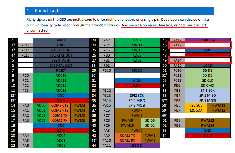
that “blank” area is the ALTERNATE FUNCTION. For example, PA13 is fine as a GPIO, and has no alternate function. The pin under PA7, pin60, and under PB10, pin30, is one that the note really applies to.
Yes, on the G30 TH Modules these are not broken out to pins but rather two test pads. The are shortened to SD for SWDIO and SC for SWCLK. A simple test by soldering to the test pads and using them as simple button inputs I was able to use them through both the InputPort and InterruptPort classes.
I am curious of why these pins were broken out to test pads. Is it for me or is it used by GHI in the stages before .netmf is loaded and the USB debugger is functional?
MCUs are normally programmed via any type of ISP (JTAG, SWD,…). I think the bare NETMF is brought onto the chip via SWD in factory and the pads are used for programming and testing.