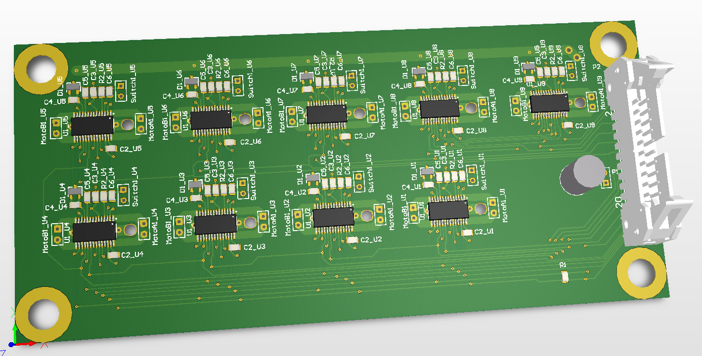
I’m creating a 9 driver L6470. I hope it works out.
3 Likes
The OCD side of me says make it symmetrical and go for 10 
1 Like
Due to cost concerns, I could not make it 10. Also, I may want to put a G80 in that last “slot”.
@Mr_John_Smith - Nice! Tell us what it is for?
Its for the robot. I’m tired of dealing with transmission line issues so I’m putting all the drivers next to each other.
@Mr_John_Smith, this might be an interesting read: StackPath
@marius, Well there is copper poured everwhere, and thermal vias, and the plate that I’m mounting it on is aluminum. I plan to either stick heat sinks on the IC or use thermal tape to the mounting plate. I may also have to use pyrolitic graphite to spread the heat out a bit faster over the mounting plate.
John regarding the communications issues you had on the longer ribbon cables, and transmission speed hell…
When they were pushing the boundaries of PATA drives ever further the UDMA standard switched cables from 40 pin to 80 pin. Every other wire in the cable was a ground. Adding 40 ground lines in addition to the 40 communications lines with the grounds interleaved between signal wires helped eliminate crosstalk by reducing capacitive coupling.
If you ever need to do a longer ribbon cable and want higher speeds, it’s an old trick worth trying. If you need to run 6 signal lines use a 12 wire cable and header and sink odd pins to ground on both sides.
As this is Altium if you set the layer stack manager with decent dimensions, you will get the proper PCB thickness in the 3D view  If 2 layer set the middle for 58 mils and then you will get a 1.6mm PCB thickness. Essential if you plan to export the PCB as a STEP file.
Is this 2 or 4 layer PCB? Hard to see the power tracks for VDD etc, so assuming they are on the underside?
Going by the names of each part you used the sheet design feature so you only had to design the circuit for each stage once.  I’ve used this once in the past and it’s very handy for designs like this.
To be honest, I just did the initial design. I paid a guy on fiver to do the layout.
@Dave_McLaughlin, yes I did use the sheet design feature; nice catch!
Top Layer
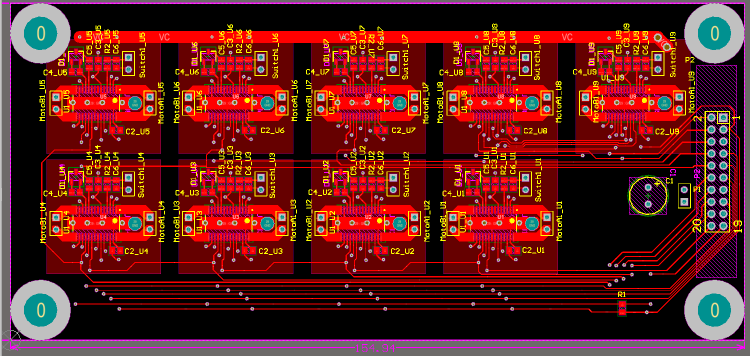
Bottom Layer

P.S. Already sent it off to Seeed Studio for fabrication. Hope the design works.
1 Like
@trent1098s, Yea, Dave mentioned that method to Gus some long time ago. I was using a 10 pin connector, with the even pins as signal and the odd pins as something else. Unfortunately, the some things else included the CK signal. I fear that noise was leaking from that pin to into the driver signals. Between that and the impedance mismatches (which I saw as voltage overshoots on the scope), I just decided to abandon the cable method and go back to this driver array method. The upsides are obvious, but the down side is that it will be a single, large irreparable part. If one driver blows there is no good way to fix it.
@Mr_John_Smith, wow pyrolitic graphite. That stuff is not cheap, so I take it that this is no normal robot either?
I don’t think it’s too expensive.
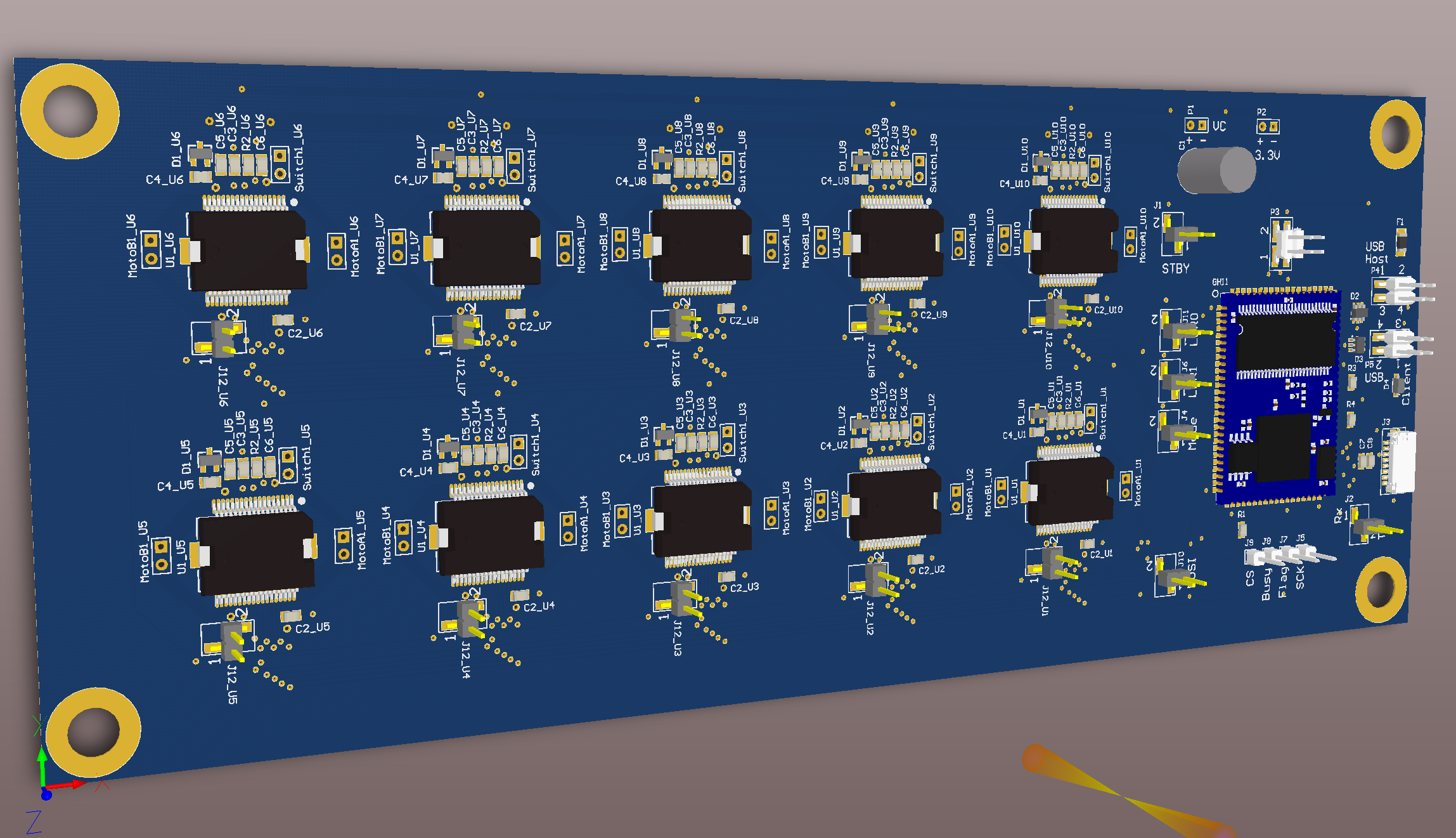
Updated the PCB with the L6470PD chip. I calculated that the L6480 would have added $500 USD to the sale price, and I can’t do that without a very good reason.
Edit your layer with the layer stack manager and your PCB will show the correct thickness in the 3D view. Important to do this if you ever export this as a STEP model for import to any mechanical CAD software. If this is 2 later, make the middle 58mills and this will give you a 1.6mm PCB. For 4 layer I use a DFRobot stack I preload each time.
I’ll do that Dave,
PS @Justin, I literally added that 10th driver just because you wanted it to be neat. I have no idea what I’m going to use it for. A spare perhaps?
3 Likes

Is that 4 layer? Looks very pale looking for a 4 layer board
Its a 2 layer board.
1 Like